- 您现在的位置:买卖IC网 > Sheet目录337 > LE25S40MB-AH (ON Semiconductor)IC MEM 4MBIT SERIAL FLASH 8SOP
LE25S40MB
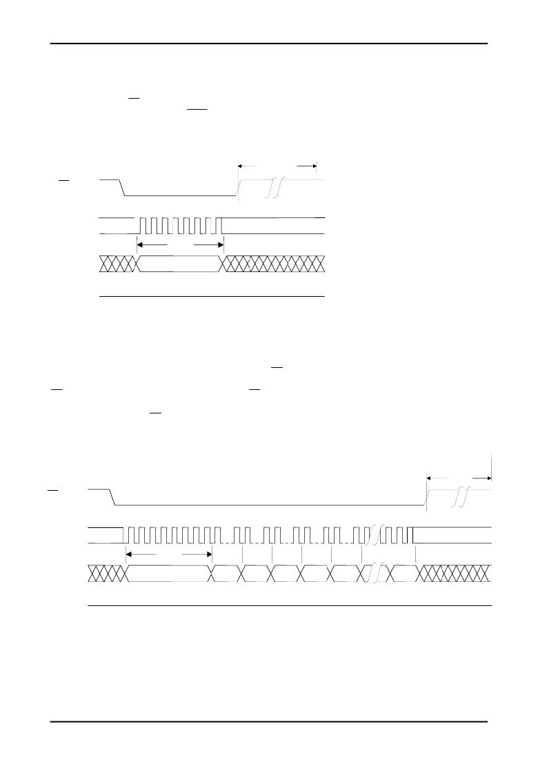
8. Chip Erase
Chip erase is an operation that sets the memory cell data in all the sectors to "1". "Figure 13 Chip Erase" shows the
timing waveforms, and Figure 20 shows a chip erase flowchart. The chip erase command consists only of the first bus
cycle, and it is initiated by inputting (60h) or (C7h). After the command has been input, the internal erase operation
starts from the rising CS edge, and it ends automatically by the control exercised by the internal timer. Erase end can
also be detected using status register RDY.
Figure 13 Chip Erase
Self-timed
Erase Cycle
tCHE
CS
Mode3
0 1 2 3 4 5 6 7
SCK
Mode0
8CLK
SI
SO
60h / C7h
MSB
High Impedance
9. Page Program
Page program is an operation that programs any number of bytes from 1 to 256 bytes within the same sector page (page
addresses: A18 to A8). Before initiating page program, the data on the page concerned must be erased using small
sector erase, sector erase, or chip erase. "Figure 14 Page Program" shows the page program timing waveforms, and
Figure 21 shows a page program flowchart. After the falling CS, edge, the command (02H) is input followed by the 24-
bit addresses. Addresses A18 to A0 are valid. The program data is then loaded at each rising clock edge until the rising
CS edge, and data loading is continued until the rising CS edge. If the data loaded has exceeded 256 bytes, the 256
bytes loaded last are programmed. The program data must be loaded in 1-byte increments, and the program operation is
not performed at the rising CS edge occurring at any other timing.
Figure 14 Page Program
Self-timed
Program Cycle
tPP
CS
Mode3
0 1 2 3 4 5 6 7 8
15 16
23 24
31 32
39 40
47
2079
SCK
Mode0
8CLK
SI
02h
Add.
Add.
Add.
PD
PD
PD
MSB
SO
High Impedance
No.A2096-12/22
发布紧急采购,3分钟左右您将得到回复。
相关PDF资料
LE25U20AMB-AH
IC MEM 2MBIT SERIAL FLASH 8SOP
LFDAS12XSIT
HARDWARE MC9S12XS 112-PIN
LFXP10E-L-EV
BOARD EVAL LATTICEXP10E STD
LH28F008SCHT-TE
IC FLASH 8MBIT 85NS 40TSOP
LH28F160S3HNS-TV
IC FLASH 16MBIT 100NS 56SSOP
LH28F160S5HNS-S1
IC FLASH 16MBIT 70NS 56SSOP
LH28F320S3HNS-ZM
IC FLASH 32MBIT 110NS 56SSOP
LH28F320SKTD-ZR
IC FLASH 32MBIT 70NS 48TSOP
相关代理商/技术参数
LE25S40QES00-AH
制造商:ON Semiconductor 功能描述:S-FLASH MEMORY(4M) - Tape and Reel
LE25S67EKS-GD0000
制造商:Legacy Electronics Inc 功能描述:512MB PC2-5300 CL5 DIMM - Bulk
LE25S80MB-AH
制造商:ON Semiconductor 功能描述:8M BIT SERIAL FLASH MEMOR - Tape and Reel 制造商:ON Semiconductor 功能描述:Flash 制造商:ON Semiconductor 功能描述:REEL - 8M BIT SERIAL FLASH MEMOR
LE25S81MCTWG
制造商:ON Semiconductor 功能描述:8M BIT SERIAL FLASH MEMOR - Tape and Reel 制造商:ON Semiconductor 功能描述:REEL - 8M BIT SERIAL FLASH MEMOR
LE25SS53DKE-CAR
制造商:Legacy Electronics Inc 功能描述:512MB PC2-4200 (533 MHZ) CL4-4-4,200 PIN SODIMM GOLD 1.181" - Bulk
LE25U20AMB
制造商:SANYO 制造商全称:Sanyo Semicon Device 功能描述:2M-bit (256K??8) Serial Flash Memory
LE25U20AMB-AH
功能描述:闪存 S-FLASH MEMORY(2M)
RoHS:否 制造商:ON Semiconductor 数据总线宽度:1 bit 存储类型:Flash 存储容量:2 MB 结构:256 K x 8 定时类型: 接口类型:SPI 访问时间: 电源电压-最大:3.6 V 电源电压-最小:2.3 V 最大工作电流:15 mA 工作温度:- 40 C to + 85 C 安装风格:SMD/SMT 封装 / 箱体: 封装:Reel
LE25U20AMBM02-AH
功能描述:闪存 RoHS:否 制造商:ON Semiconductor 数据总线宽度:1 bit 存储类型:Flash 存储容量:2 MB 结构:256 K x 8 定时类型: 接口类型:SPI 访问时间: 电源电压-最大:3.6 V 电源电压-最小:2.3 V 最大工作电流:15 mA 工作温度:- 40 C to + 85 C 安装风格:SMD/SMT 封装 / 箱体: 封装:Reel
